
-
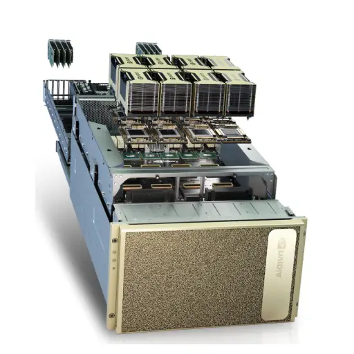 NVIDIA DGX H100 ( 8×H100 SXM5 AI Supercomputing Platform )
USD832,000
-
 NVIDIA RTX A5000
Rated 4.67 out of 5USD15,200
-
 AI Bridge TS2-08 (8 Channel Analytics Device)
USD5,760
-
 HGX H100 Optimized X13 8U 8GPU Server: The Ultimate AI and HPC Powerhouse for Exascale Computing
USD480,000
-
 NVIDIA H100 80GB PCIe Tensor Core GPU
USD51,200Original price was: USD51,200.USD49,600Current price is: USD49,600. -
 AI Bridge LTE TS2-08: The Ultimate 8/16-Channel Edge AI Analytics Powerhouse with LTE & GPS
USD7,200
Products Mentioned in This Article


NVIDIA B200 Blackwell Architecture
In 2026, if you are evaluating enterprise AI infrastructure, one name consistently dominates the conversation: Blackwell.
NVIDIA’s latest architecture, succeeding Hopper (H100/H200), is not just an incremental upgrade. it represents a fundamental redesign of how AI processors are built and scaled.
At the center of this architecture is the B200 GPU, which powers systems like the DGX B200 equipped with 8 GPUs, positioning it among the most powerful commercial AI machines available today.
But what exactly makes Blackwell so significant? Why did NVIDIA move away from its long-standing “bigger single chip” strategy? And most importantly, what do these architectural changes mean if you are making a real purchasing decision for DGX systems?
This guide breaks it all down in a clear and practical way.
Why NVIDIA Needed Blackwell
To understand Blackwell, you first need to understand the problem it was designed to solve. Until 2023, NVIDIA’s scaling strategy was straightforward: each new generation meant a larger chip with more transistors, more memory, and higher compute density.
But this approach eventually hit a physical wall. In modern semiconductor manufacturing, the reticle limit defines the maximum size of a single chip die — roughly 858 mm² in TSMC’s advanced process. The H100, at about 814 mm², was already very close to this limit. At that point, further scaling by simply increasing die size was no longer feasible.
At the same time, AI models were scaling in the opposite direction. Large language models were doubling in size every few months, moving from systems like GPT-4 (around 1.8 trillion parameters) toward next-generation frontier models approaching 10 trillion parameters. These models demand exponentially more compute power and memory bandwidth than a single monolithic GPU can efficiently deliver.
Blackwell introduces a shift in philosophy. Instead of building a single larger chip, NVIDIA combines two GPU dies into one tightly integrated logical unit. This chiplet-based approach enables scaling beyond the physical limits of a single die while maintaining high performance and efficiency. While chiplet designs have been widely used in CPUs — most notably by AMD — Blackwell marks NVIDIA’s first major adoption of this architecture in flagship AI accelerators.
Dual-Die Architecture — The Core of Blackwell
Each B200 GPU is built from two separate silicon dies, manufactured using TSMC’s 4NP process (an enhanced variant of the 5nm-class node). These two dies are connected through a high-speed internal link called NV-HBI (NVIDIA High Bandwidth Interface), delivering up to 10 TB/s of interconnect bandwidth.
At this level of bandwidth, the system behaves as a single unified GPU from a software perspective. Developers do not need to explicitly manage workload distribution between the dies — the architecture abstracts that complexity away entirely.
From an engineering standpoint, this is a significant breakthrough. In traditional chiplet-based designs (such as AMD EPYC CPUs), inter-chip communication introduces measurable latency, and software must often account for data locality and scheduling overhead. In Blackwell, NV-HBI reduces this gap so dramatically that the inter-die latency drops to just a few nanoseconds — effectively approaching the behavior of a monolithic chip.
Each die in the B200 contains approximately 104 billion transistors, resulting in a combined total of 208 billion transistors per GPU. For comparison, the H100 featured around 80 billion transistors, meaning Blackwell delivers roughly 2.6× more transistor density.
This increase directly translates into higher counts of CUDA cores, Tensor cores, and significantly expanded on-chip memory bandwidth — forming the foundation for Blackwell’s performance leap in large-scale AI workloads.
HBM3e Memory — A Jump to 192GB
Surrounding this dual-die package is a stack of 8 HBM3e memory modules, delivering a total of 192 GB of high-bandwidth memory with up to 8 TB/s of memory bandwidth. This represents a 36% increase in capacity and a 67% increase in bandwidth compared to H200.
To understand what this means in practice, consider a real-world example. The Llama 3 405B model requires roughly 800 GB of FP16 memory to run efficiently. On an H100 (80 GB), this workload must be distributed across around 10 GPUs. On an H200 (141 GB), it still requires about 6 GPUs. On the B200, with 192 GB of memory, the same model can run on just 4 to 5 GPUs.
This reduction in GPU count is not just a cost optimization — it significantly reduces system complexity, interconnect overhead, and synchronization latency during training and inference.
The 8 TB/s memory bandwidth is equally critical. In large language models, performance is often not limited by raw compute, but by memory bandwidth. Each generated token requires streaming a large portion of model weights from memory. As a result, the B200 can generate significantly more tokens per second than the H200 for the same model, simply because it can feed data to the compute units faster and more efficiently.
Fifth-Generation Tensor Cores and FP4 Format
One of the most important changes in Blackwell is the introduction of FP4 precision in its fifth-generation Tensor Cores. This new 4-bit format (including E2M1 and E3M0 variants) is designed to drastically reduce memory usage and increase computational efficiency while maintaining acceptable accuracy through careful quantization techniques.
On paper, each B200 GPU delivers up to 9 petaflops of FP4 performance, a massive figure that did not exist in the H200 architecture at all, since Hopper does not support FP4. In FP8 precision — which is supported by both generations — the improvement is more modest: around 4.5 petaflops for B200 versus ~4 petaflops for H200, roughly a 12% gain in raw FP8 compute.
This distinction is critical: most of Blackwell’s performance leap does not come from traditional compute scaling, but from the introduction of lower-precision data formats like FP4.
For DGX buyers, this has direct implications. If your workloads are not optimized for FP4, you are effectively not accessing the primary advantage of Blackwell hardware. By late 2026, major frameworks such as PyTorch, TensorRT-LLM, and vLLM are expected to support FP4, but the level of maturity and stability varies across use cases.
For inference workloads, FP4 is already highly effective, with minimal and often acceptable accuracy loss. For training, however, FP4 remains less stable for many models, and most real-world training pipelines still rely on FP8 or BF16 precision.
Second-Generation Transformer Engine
In Hopper, NVIDIA introduced the Transformer Engine, a dynamic system that automatically switched between FP8 and FP16 precision depending on the sensitivity of each computation layer. This allowed a balance between performance and numerical stability in large language models.
With Blackwell, this engine evolves into a second-generation Transformer Engine, now extending support to FP4 precision and incorporating more advanced precision management algorithms.
Instead of using a single precision mode across a model, the system dynamically selects precision at a much finer granularity — sometimes per layer, and in certain cases even per tensor. Highly sensitive layers remain in FP16, dense compute-heavy layers typically run in FP8, and certain attention operations that are more tolerant to quantization can be executed in FP4.
The result is a system that effectively delivers FP4-level performance while preserving model accuracy through intelligent precision routing.
However, from a buyer’s perspective, this is heavily dependent on NVIDIA’s software stack. These optimizations are not automatically available in standard PyTorch implementations. Without NVIDIA’s Transformer Engine integration, much of this performance advantage is not realized. This significantly increases the strategic importance of the NVIDIA AI Enterprise ecosystem in DGX B200 deployments.
Buy NVIDIA DGX GB200 NVL72
NVLink Generation 5 — Faster On-Node Scaling
In DGX B200 and other Blackwell-based systems, NVLink Gen5 doubles GPU-to-GPU bandwidth to approximately 1.8 TB/s bidirectional, compared to around 900 GB/s in the previous generation (H100/H200 systems).
This enables 8 GPUs inside a DGX B200 to behave more like a single unified GPU domain with approximately 1.5 TB of aggregate bandwidth, dramatically reducing synchronization overhead in multi-GPU training and inference.
Even more importantly, NVIDIA introduces the NVLink Switch System, which reaches its full scale in larger platforms like the GB200 NVL72. This allows up to 72 GPUs to operate within a single high-speed NVLink domain, compared to the 8-GPU limit in DGX H200 systems.
For large model training, this is a major architectural shift. In Hopper-based systems, any workload exceeding 8 GPUs must rely on InfiniBand for cross-node communication, which is significantly slower — often by an order of magnitude or more compared to NVLink. In Blackwell systems, scaling can remain within a unified high-speed NVLink fabric across dozens of GPUs, dramatically improving efficiency for large-scale distributed training.
Real-World Performance Comparison — Benchmark Numbers
NVIDIA claims that the B200 delivers up to 30× higher inference performance and up to 4× faster training compared to H100. At first glance, these numbers look extremely impressive — but they require careful interpretation.
The 30× inference claim comes from a very specific scenario: GPT-MoE-1.8T running on GB200 NVL72 in FP4, compared against H100 in FP8. This is not a like-for-like comparison — multiple variables change at once, including hardware generation, precision format, and system scale.
When normalized to a fair comparison (B200 vs H200, both running FP8 on similar model sizes like 70B), the real-world improvement is typically around 2× to 2.5×.
If FP4 is enabled on B200 while H200 remains limited to FP8 (its best-supported precision), performance gains can reach 3× to 4×, depending on workload characteristics and model architecture.
For training workloads, B200 generally delivers 2× to 3× faster performance compared to H200, assuming FP8 with the second-generation Transformer Engine is fully utilized. However, if training relies on BF16 — which is still common in many research pipelines — the improvement drops to around 1.3× to 1.5×.
For fine-tuning and RAG workloads, performance gains typically fall in the 2× to 4× range, largely driven by higher memory bandwidth and faster inference throughput.
Practical takeaway
If a vendor claims “30× faster performance,” it should be treated with caution. In realistic production scenarios, a 2× to 4× improvement over H200 is a more accurate expectation depending on workload optimization and precision usage.
Blackwell Infrastructure Challenges
The architectural leap in Blackwell also introduces new infrastructure requirements that buyers must seriously consider.
Power
A single DGX B200 consumes up to 14.3 kW. At rack scale (e.g., 4 systems per rack), this can exceed 57 kW per rack. Most existing data centers are not designed for this density. Electrical upgrades alone can cost $50K to $200K per rack, depending on facility readiness.
Cooling
While DGX B200 remains air-cooled, larger Blackwell systems like GB200 NVL72 require liquid cooling by design. Even for DGX B200 clusters, liquid cooling is often recommended at scale. Retrofitting cooling infrastructure can easily become a six-figure investment per site.
Networking
To fully utilize Blackwell in multi-node setups, InfiniBand NDR (400 Gb/s) or higher is required. Legacy networking infrastructure quickly becomes a bottleneck and can severely limit scaling efficiency.
Software maturity
Although the Blackwell ecosystem is rapidly maturing toward late 2026, it is still not as battle-tested as Hopper (H200). Some frameworks, kernels, and optimization libraries are not yet fully optimized. Early adopters should expect a transition period with occasional performance tuning challenges that are no longer present in H200-based deployments.
Final Conclusion
Blackwell is undeniably a milestone architecture that will shape the future of AI computing. Innovations such as chiplet-based design and FP4 precision are not just incremental upgrades—they represent a fundamental shift that will define the next generation of AI hardware.
For organizations with large-scale workloads, strong budgets, and mature infrastructure, investing in DGX B200 is a forward-looking decision that aligns with next-generation AI demands.
However, for most mid-sized enterprises, DGX H200 remains the optimal balance point. It delivers exceptional performance with greater software maturity, broader availability, lower total cost, and significantly simpler infrastructure requirements.
If your workloads are production-ready and stable, and your priority is cost-efficiency and operational reliability, H200 is still the most economically rational choice in 2026. On the other hand, if you are building a next-generation AI platform designed to scale toward 2030 and beyond—and you already have the infrastructure and expertise—then B200 becomes a strategic long-term investment.
Ultimately, the right decision is not driven by which architecture looks more impressive in NVIDIA’s presentations. It depends on ROI, team maturity, infrastructure readiness, and your real-world deployment timeline.
Last update at December 2025